
Super-Efficient Microcomb Technology
Breakthrough photonic molecular architecture delivering >60% conversion efficiency for next-generation optical interconnects
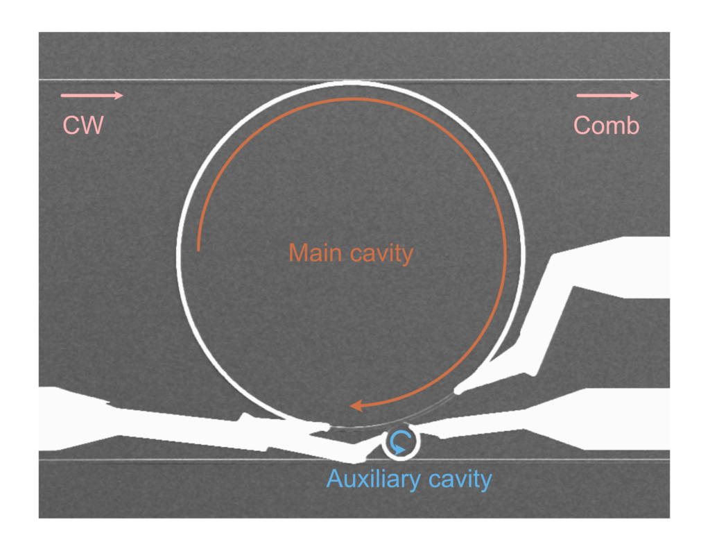
Photonic Molecular Architecture
Our patented super-efficient microcomb technology revolutionizes multiwavelength laser systems with unprecedented efficiency and reliability
Revolutionary Efficiency Breakthrough
Our photonic molecular design enables coherent multiwavelength generation with minimal power consumption, achieving >60% conversion efficiency compared to the industry standard of less than 5%. This can match or exceed mode-locked lasers with wall-plug efficiencies of 11%-15%.
Technical Specifications
Industry-leading performance metrics that redefine what’s possible in optical communications
|
Feature
|
Solinide
|
Soliton Microcombs
|
Laser Arrays
|
|
Conversion Efficiency |
>60% |
<5% |
20-30% |
|
Number of Wavelengths |
100+ |
100+ |
Limited |
|
Power per Line |
>1mW |
<0.1mW |
>1mW |
|
Thermal Stability |
Excellent |
Excellent |
Poor |
|
Spectral Uniformity |
<4dB |
~10dB |
<4dB |
|
Total Power Consumption |
<2W |
~5W |
~4.5W |
|
CMOS Compatible |
Yes |
Yes |
No |
|
Feature
|
Solinide
|
Soliton Microcombs
|
Laser Arrays
|
|
Wall-Plug Efficiency |
45% |
<5% |
10% |
|
Number of Wavelengths |
100+ |
100+ |
Limited |
|
Power per Line |
>1mW |
<0.1mW |
1mW |
|
Thermal Stability |
Excellent |
Good |
Poor |
|
Spectral Uniformity |
<5dB |
~10dB |
<5dB |
|
Total Power Consumption |
<1W |
~5W |
~10W |
|
CMOS Compatible |
Yes |
Yes |
No |
Products
Publications
World-leading research backed by strong intellectual property
Silicon Nitride Photonics Solving Critical Infrastructure Challenges
From hyperscale datacenters to quantum networks, Solinide’s 60%+ optical efficiency enables next-generation computing and telecommunications infrastructure.
Hyperscale Datacenters
Powering the World’s Largest Digital Infrastructure
AI Infrastructure
Enabling Exascale AI Training and Inference
5G/6G Networks
Future-Proofing Mobile Network Infrastructure
Quantum Communications
Building the Quantum Internet
Edge Computing
Bringing Datacenter Performance to the Edge
HPC Clusters
Breaking the Petaflop Interconnect Barrier
One Platform. Multiple Breakthrough Applications.
Solinide’s silicon nitride photonics technology delivers transformative efficiency gains across the entire digital infrastructure ecosystem. Our 60%+ optical conversion efficiency, a 10x improvement over silicon photonics, translates directly to:
Reduced Capital Expenditure
Higher performance per watt means fewer servers, switches, and cooling systems to achieve the same computational throughput.
Lower Operating Costs
Dramatically reduced power consumption and cooling requirements cut datacenter OPEX by up to 10%.
Increased Deployment Density
Lower thermal output enables higher rack density, improving datacenter space utilization and reducing real estate costs.
Extended Equipment Lifespan
Reduced thermal stress on components increases MTBF and lowers replacement cycles.
Faster Time-to-Market
Standards-compliant packaging and integration flows minimize design-in time for OEMs and system integrators.
Future-Proof Architecture
Platform scales from today’s 800G requirements to tomorrow’s multi-terabit demands without fundamental redesign.
Frequently Asked Questions
Ready to Transform Your Infrastructure?
Whether you’re architecting hyperscale datacenters, building AI supercomputers, or deploying 6G networks, Solinide’s silicon nitride photonics delivers the efficiency breakthrough that makes exponential scaling economically viable.
Our team brings decades of experience in photonic integration, datacenter architecture, and telecommunications infrastructure. We work closely with forward-thinking organizations to validate our technology in real-world deployments.